 |
Dot-matrix liquid crystal display (LCD) |
Main Frame (acces to all the site)
|
Dot-matrix liquid crystal display (LCD) |
2. Terminal Functions
Table 1. Terminal functions
|
Signal name
|
No. of
terminals |
I/O
|
Destination
|
Function
|
|
DB0
to DB3
|
4
|
I/O
|
MPU
|
Tristate
bidirectional lower four data buses: data is read from the module to the
MPU or written to the module from the MPU through the buses. If the interface
data is 4 bits, this signals are not used.
|
|
DB4
to DB7
|
4
|
I/O
|
MPU
|
Tristate
bidirectional upper four data buses: data is read from the module to the
MPU or written to the module from the MPU through the buses. DB7
is also used as a busy flag.
|
|
E
|
1
|
Input
|
MPU
|
Operation
start signal: the signal activates data write or read.
|
|
R/-W
|
1
|
Input
|
MPU
|
Read (R)
and write (-W) selections signals:
- 0 : Write
- 1 : Read |
|
RS
|
1
|
Input
|
MPU
|
Register
selection signals:
- 0: Instruction register (Write); Busy Flag and address counter (Read) - 1: Data register (Write and Read) |
|
VLC
|
1
|
-
|
Power supply
|
Power supply
terminal for driving liquid crystal display. The scrin contrast can be
varied by changing VLC
|
|
VDD
|
1
|
-
|
Power
supply
|
+5 V
|
|
VSS
|
1
|
-
|
Power
supply
|
Ground terminal:
0V
|
3. Basic Operations
3.1 Registers
The controler has two kinds
of eight-bit registers: the instruction register (IR) and the data register
(DR). They are selected by the register select (RS) signals as shown in Table
2.
The IR store instruction codes such as Display Clear
and Cursor Shift, and the addres information of display data RAM (DD RAM) and
character generator RAM (CG RAM). They can be writen from the MPU, but cannot
be read to the MPU.
The DR temporarily stores data to be written into DD
RAM or CG RAM, or read from DD RAM or CG RAM. When data written into DD RAM
or CG RAM from the MPU, the data in the DR is automatically writen into DD RAM
or CG RAM by internal operation. However, when data is read from DD RAM or CG
RAM, the necesary data addres is writen into the IR. The specified data is read
out to the DR and then the MPU reads it from the DR. After the read operation,
the next adress is set and DD RAM or CG RAM data at the addres is read into
thr DR for the next read operation.
Table 2. Register selection
|
RS
|
R/-W
|
Operation
|
|
0
|
0
|
IR selection, IR write Internal operation: Display clear |
|
0
|
1
|
Busy flag (DB7) and address counter (DB0 to DB6) read |
|
1
|
0
|
DR selection, DR write. Internal operation: DR to DD RAM or CG RAM |
|
1
|
1
|
DR selection, DR read. Internal operation: DD RAM or CG RAM to DR |
3.2 Busy flag (BF)
The flag indicate whether the module is ready to accept the next instruction. As show in table 2, the signal is output to DB7 if RS = 0 and R/-W = 1. If the value is 1, the module is working internally and the instruction cannot be accepted. If the vlue is 0, the next instruction can be written. Therefore, the flag statusneeds to be checked before executing an instruction. If an instruction is executed without checking the flag status, wait for more than the execution time show in Table 5. Instruction Outline.
3.3 Address counter (AC)
The counter specifies an address writen when data is written into DD RAM or CG RAMand the data stored in DD RAM or CG RAM is read out. If an Address Set instriction (for DD RAM or CG RAM) is written in the IR, the addresinformation is transferred from the IR to the AC. When display data is written into or read from DD RAM or CG RAM, the AC is automatically incremented or decremented by one according to the Entry Mode Set. The contents of the AC are output to DB0 to DB6 as show in Table 2 if RS = 0 and R/-W = 1.
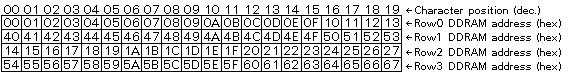
3.4 Display data RAM (DD RAM)
DD RAM has a capacity of up to
80 x 8 bits and stores display data of 80 eight-bit characters codes. Some storage
areas of DD RAM which are not used for display can be used as general data RAM.
The DD RAM address and the displayy digits of the LCD
panel correspond as follows.
If the display is shifted,
DD RAM address 00h to 27h are displayed in digits from the first line and 40h
to 67h in the second line (from a LCD with two line).
![]()

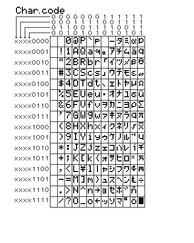
3.5 Character generator ROM (CG ROM)
Character generator ROM generates 192
types of 5 x 7 dot matrix character patterns from eight-bit character codes.
Table 3 shows the correspondence between the CG ROM character
codes and characters patterns.
Table 3.
3.6 Character generator RAM (CG RAM)
CG RAM is used to create character
patterns freely by programming. Eight types of character patterns can be written.
Table 4 shows the character patterns created from CG RAM addresses
and data. To display a created character pattern, the character code in the
left column of the table is written into DD RAM corresponding to the display
position (digit). The area not used for display
are available as general data RAM.
|
Character code
(DD RAM data) |
CG RAM address
|
Character pattern
(CG RAM data) |
|
|
7 6 5 4 3 2 1 0
|
5 4 3 2 1 0
|
7 6 5 4 3 2 1 0
|
|
|
0 0 0 0 x 0 0 0
|
0 0 0
0 0 1 0 1 0 0 1 1 0 0 0 1 0 0 1 0 1 1 1 0 1 1 1 |
x x x 1 1 1 1 0
x x x 1 0 0 0 1 x x x 1 0 0 0 1 x x x 1 1 1 1 0 x x x 1 0 1 0 0 x x x 1 0 0 1 0 x x x 1 0 0 0 1 x x x 0 0 0 0 0 |
Example of character pattern (R)
|
|
0 0 0 0 x 0 0 1
|
0 0 0
0 0 1 0 1 0 0 1 1 0 0 1 1 0 0 1 0 1 1 1 0 1 1 1 |
x x x 1 1
1 0 1
x x x 0 1 0 1 0 x x x 1 1 1 1 1 x x x 0 0 1 0 0 x x x 1 1 1 1 1 x x x 0 0 1 0 0 x x x 0 0 1 0 0 x x x 0 0 0 0 0 |
Example of character pattern (¥)
|
|
...
|
...
|
...
|
...
|
|
0 0 0 0 x 1 1 1
|
0 0 0
0 0 1 0 1 0 0 1 1 1 1 1 1 0 0 1 0 1 1 1 0 1 1 1 |
Notes:
- In CG RAM data, 1 corresponds to Selection and 0 to Non-selection on the display.
- Character code bits 0 to 2 and CG RAM address bits 3 to 5 correspond with each other (three bits, eight types).
- CG RAM address bits 0 to 2 specify a line position for a character pattern. Line 8 of a character pattern is cursor position where the logical sum of the cursor and CG RAM data is displayed. Set the data of line 8 to 0 to display the cursor. If the data is changed to 1, one bit lights, regardless of the cursor.
- The character pattern column position correspond to CG RAM data bits 0 to 4 and bit 4 comes to the left end. CG RAM data bits 5 to 7 are not displayed but can be used as general data RAM.
- When reading a character pattern from CG RAM, set to 0 all of character code bits 4 to 7. Bits 0 to 2 determine which pattern will be read out. Since bit 3 is not valid, 00h and 08h select the same character.
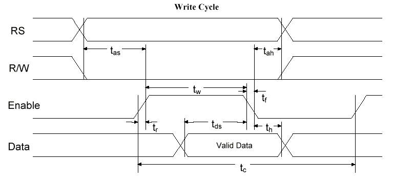
4. Timing Characteristics
4.1 Write timing characteristics
|
Item
|
Symbols
|
Standard
|
Units
|
|||
|
Max. |
|||||
| Enable cycle time |
tc
|
1000
|
-
|
ns
|
||
| Enable pulse width |
High level
|
tw
|
450
|
-
|
ns
|
|
| Enable rise and fall time |
tr, tf
|
-
|
25
|
ns
|
||
| Setup time |
RS,R/-W -› E
|
tas
|
140
|
-
|
ns
|
|
| Address hold time |
tah
|
10
|
-
|
ns
|
||
| Data setup time |
tds
|
195
|
-
|
ns
|
||
| Data hold time |
th
|
10
|
-
|
ns
|
||
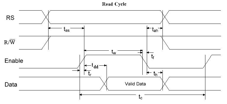
4.2 Read timing characteristics
|
Item
|
Symbols
|
Standard
|
Units
|
|||
|
Max. |
|||||
| Enable cycle time |
tc
|
1000
|
-
|
ns
|
||
| Enable pulse width |
High level
|
tw
|
450
|
-
|
ns
|
|
| Enable rise and fall time |
tr, tf
|
-
|
25
|
ns
|
||
| Setup time |
RS,R/-W -› E
|
tas
|
140
|
-
|
ns
|
|
| Address hold time |
tah
|
10
|
-
|
ns
|
||
| Data delay time |
tdd
|
-
|
320
|
ns
|
||
| Data hold time |
th
|
20
|
-
|
ns
|
||
5. Instructions Outline
|
Instructions
|
Code
|
Function
|
Execution
time |
|||||||||
|
RS
|
R/W
|
DB7
|
DB6
|
DB5
|
DB4
|
DB3
|
DB2
|
DB1
|
DB0
|
|||
| (1) Display clear |
0
|
0
|
0
|
0
|
0
|
0
|
0
|
0
|
0
|
1
|
Clears all display and returns cursors to home positions (address 0) |
1.64 ms
|
| (2) Cursor Home |
0
|
0
|
0
|
0
|
0
|
0
|
0
|
0
|
1
|
•
|
Returns cursor to home position. Shifted display returns to home positions and DD RAM cintents do not change |
1.64 ms
|
| (3) Entry Mode Set |
0
|
0
|
0
|
0
|
0
|
0
|
0
|
1
|
I/D
|
S
|
Sets direction of cursor movement and whether display will be shifted when data is written or read |
40 us
|
| (4) Display ON/OFF control |
0
|
0
|
0
|
0
|
0
|
0
|
1
|
D
|
C
|
B
|
Turns ON/OFF total display (D) and cursor (C), and makes cursor position column start blinking (B). |
40 us
|
| (5) Cursor/Display Shift |
0
|
0
|
0
|
0
|
0
|
1
|
S/C
|
R/L
|
•
|
•
|
Moves cursor and shifts display without changing DD RAM contents. |
40 us
|
| (6) Function Set |
0
|
0
|
0
|
0
|
1
|
DL
|
N
|
F
|
•
|
•
|
Sets interface data length (DL). |
40 us
|
| (7) CG RAM Address Set |
0
|
0
|
0
|
1
|
ACG
|
Sets CG RAM addres to start transmitting or receiving CG RAM data. |
40 us
|
|||||
| (8) DD RAM Address Set |
0
|
0
|
1
|
ADD
|
Sets DD RAM addres to start transmitting or receiving DD RAM data. |
40 us
|
||||||
| (9) BF/Addres Read |
0
|
1
|
BF
|
AC
|
Reads BF indicating module in internal operation and AC contents (used for both CG RAM and DD RAM) |
2 us
|
||||||
| (10) Data Write to CG RAM or DD RAM |
1
|
0
|
Write Data
|
Write data into CG RAM and DD RAM |
40 us
|
|||||||
| (11) Data Read from CG RAM or DD RAM |
1
|
1
|
Read Data
|
Read data into CG RAM and DD RAM |
40 us
|
|||||||
Nota:
| • - invalid bit ACG - CG RAM addres ADD - DD RAM addres |
|
5. Instruction Details
   Instruction                                 Code

                             RS  R/W DB7 DB6 DB5 DB4 DB3 DB2 DB1 DB0
                             ==  === === === === === === === === ===
Clear Display                 0   0   0   0   0   0   0   0   0   1

Return Home                   0   0   0   0   0   0   0   0   1   *

Entry Mode Set                0   0   0   0   0   0   0   1  I/D  S

Display ON/OFF                0   0   0   0   0   0   1   D   C   B

Cursor and Display Shift      0   0   0   0   0   1  S/C R/L  *   *

Function Set                  0   0   0   0   1   DL  N   F   *   *

Set CG RAM address            0   0   0   1   A   A   A   A   A   A

Set DD RAM address            0   0   1   A   A   A   A   A   A   A

Read busy flag and address    0   1   BF  A   A   A   A   A   A   A

Write data to CG or DD RAM    1   0   D   D   D   D   D   D   D   D

Read data from CG or DD RAM   1   1   D   D   D   D   D   D   D   D
Notes
* means 0 or 1 have no effect
Where execution times are given as A / B
B applies for 1/16 duty (2 display lines)
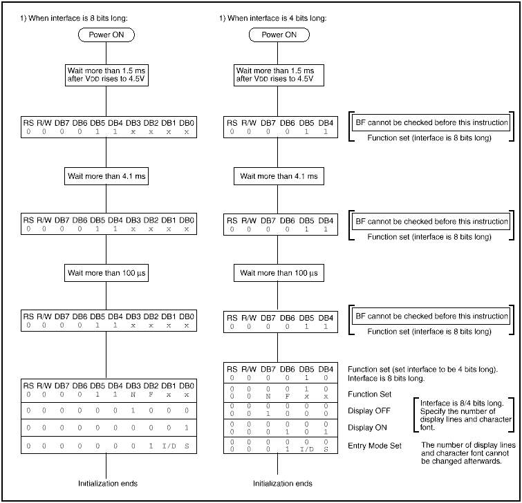
6. Example of Instruction Use (eight or four birs)